The Differences Between Scanning Electron Microscope (SEM) and Transmission Electron Microscope (TEM)
Humans rely on their senses to perceive the world, and these microscopic analysis instruments extend human perception. We are all familiar with optical microscopes, but these microscopes, which work based on lens imaging, are limited by the Abbe limit, where the resolution is limited to half the wavelength of the light used.
Therefore, the resolution of optical microscopes is only at the micrometer level due to the limitation of the wavelength of light. However, fast-moving electrons have wave-particle duality, and as a wave, an important characteristic of electrons is their wavelength.
With increasing acceleration voltage, the electron wavelength decreases. By using higher acceleration voltages, such as 30 kV, it is possible to obtain electrons with a wavelength of approximately 7 pm. Electron microscopes are created by using electrons as the "light" and substituting magnetic lenses for conventional optical lenses.
When electrons interact with a solid specimen, they produce a series of specimen-related information, including induced electromotive force, cathodoluminescence, characteristic X-rays, back-scattered electrons, Auger electrons, secondary electrons, absorbed electrons, transmitted electrons, etc. By utilizing this information, it is possible to obtain structural information at the microscopic scale.
The differences between SEM and TEM
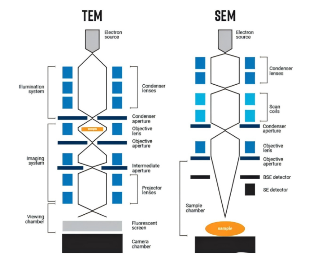
SEM (Scanning Electron Microscope) and TEM (Transmission Electron Microscope) are two common forms of electron microscopes. SEM uses Secondary Electrons (SE) and Back-scattered Electrons (BSE) to capture images of the specimen surface, while TEM detects transmitted electrons to generate projection images through the specimen's interior.
SEM scans the specimen surface with a focused electron beam and collects the signals generated at each point to construct an amplified image pixel by pixel. The scanning coil located below the objective lens guides the beam precisely through the specimen's surface in the X-Y plane. Depending on the magnification (up to 2 million times), the beam scans a field of view ranging from a few micrometers to millimeters.
Typical acceleration voltages for SEM range from 1 kV to 30 kV. Lower acceleration voltages provide a gentler beam, which is useful for imaging beam-sensitive and insulating specimens. Secondary electrons are less sensitive to atomic numbers and more suitable for observing surface topography. In contrast, backscattered electrons yield higher signals for specimens with larger atomic numbers, making them suitable for compositional imaging.
The Transmission Electron Microscope (TEM) typically operates at acceleration voltages between 30 kV and 300 kV, which are significantly higher than those used in SEM instruments.
This high accelerating voltage enables TEM to achieve exceptionally high image resolution.
In particular, Corrected Aberration TEMs can reach spatial resolutions below 1 Ångström (1 Å = 0.1 nm), allowing scientists to observe atomic-level details such as the arrangement of individual atoms within nanoparticles.
In the imaging process, the electron beam is expanded into a broad, uniform beam that passes through the specimen.
Unlike SEM, which scans the electron beam point by point using scanning coils, TEM employs an illumination system that produces a wide and stable beam covering the entire specimen area simultaneously.
TEM can achieve magnifications exceeding 50 million times (50,000,000×), enabling direct visualization of the atomic crystal structure of materials.
However, specimens used for TEM analysis must be extremely thin — typically less than 100 nanometers — to allow the electron beam to transmit through them.
The transmitted electrons in TEM can be divided into several categories, such as:
Direct Beams – electrons that pass straight through the specimen
Diffracted Beams – electrons that are scattered at specific angles due to atomic lattice interactions
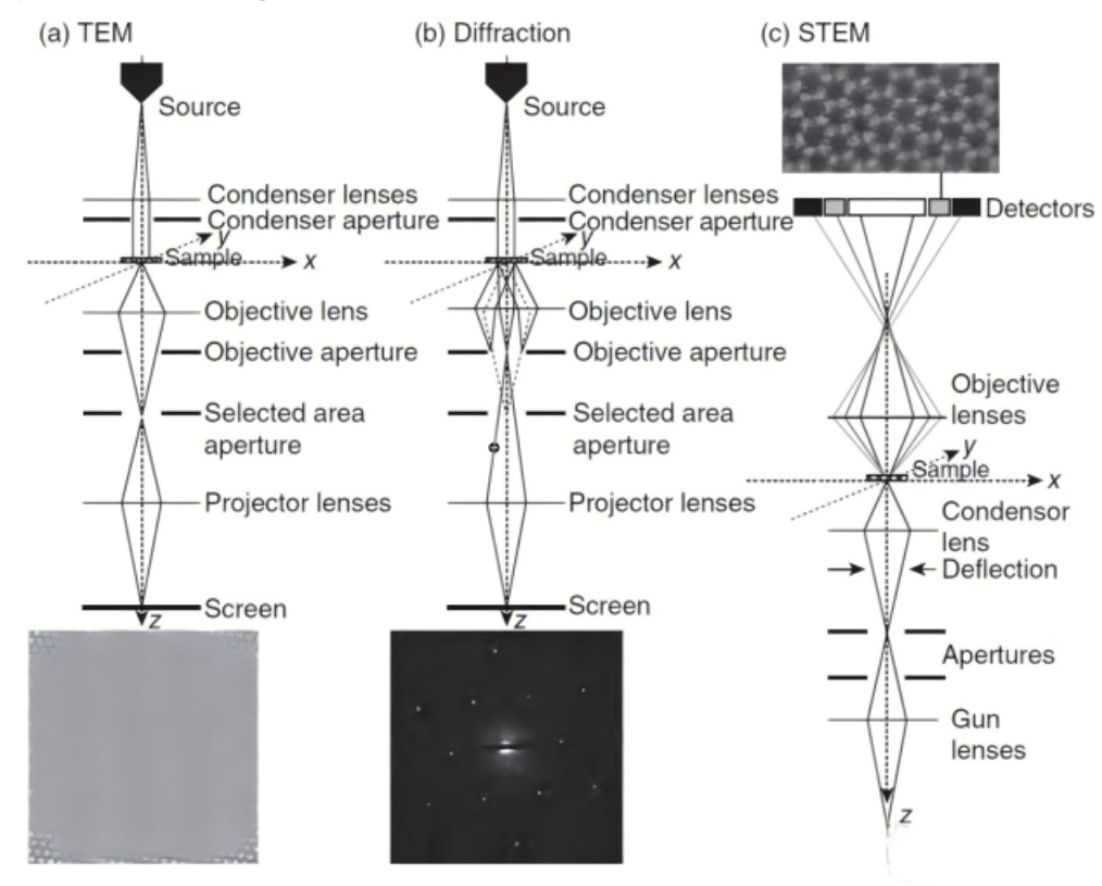
These lead to two main imaging modes: Imaging Mode and Diffraction Mode.
In Diffraction Mode, the Intermediate Lens and Objective Aperture located below the specimen can be adjusted to form images based on specific diffraction patterns, providing valuable insight into the crystal structure and defects within materials.
✅ Key Highlights of TEM
High accelerating voltage (30 – 300 kV) → Enables atomic-level resolution
Non-scanning beam → Produces projection images in a single frame
Extremely high magnification (> 50 million ×)
Requires ultrathin specimens (< 100 nm)
Supports both Imaging Mode and Diffraction Mode for analyzing crystal structure and material defects
The Scanning Transmission Electron Microscope (STEM) operates on similar principles to the Transmission Electron Microscope (TEM) but incorporates additional systems such as scanning coils, signal detectors, and electronic control circuits. These enhancements allow the instrument to scan the electron beam across the specimen in a highly precise and systematic manner.
In STEM mode, the electron beam is focused into an extremely fine probe — typically with a spot size ranging from 0.05 to 0.2 nanometers — and scanned across the specimen in a raster grid pattern. The electron beam, aligned parallel to the optical axis, illuminates each point on the specimen sequentially while detectors collect signal data from every scanned position.
In essence, STEM combines the advantages of both SEM and TEM:
from TEM, it inherits the ability to detect transmitted electrons that provide internal structural information;
and from SEM, it adopts the principle of point-by-point scanning, which enables the acquisition of high-resolution spatial and signal information at the atomic scale.
Modern STEM systems are equipped with multiple detectors placed around the specimen to capture different signal types, such as:
Annular Dark Field (ADF) Detectors, which collect scattered electrons at low to medium angles;
High-Angle Annular Dark Field (HAADF) Detectors, used for Z-contrast imaging, where image brightness correlates with atomic number;
Bright Field (BF) Detectors, which capture directly transmitted electrons at the beam center.
Because of this versatility, STEM serves as a powerful analytical tool that allows both structural imaging and compositional or crystallographic analysis to be performed simultaneously at the atomic level.