What is a Scanning Electron Microscope (SEM)?
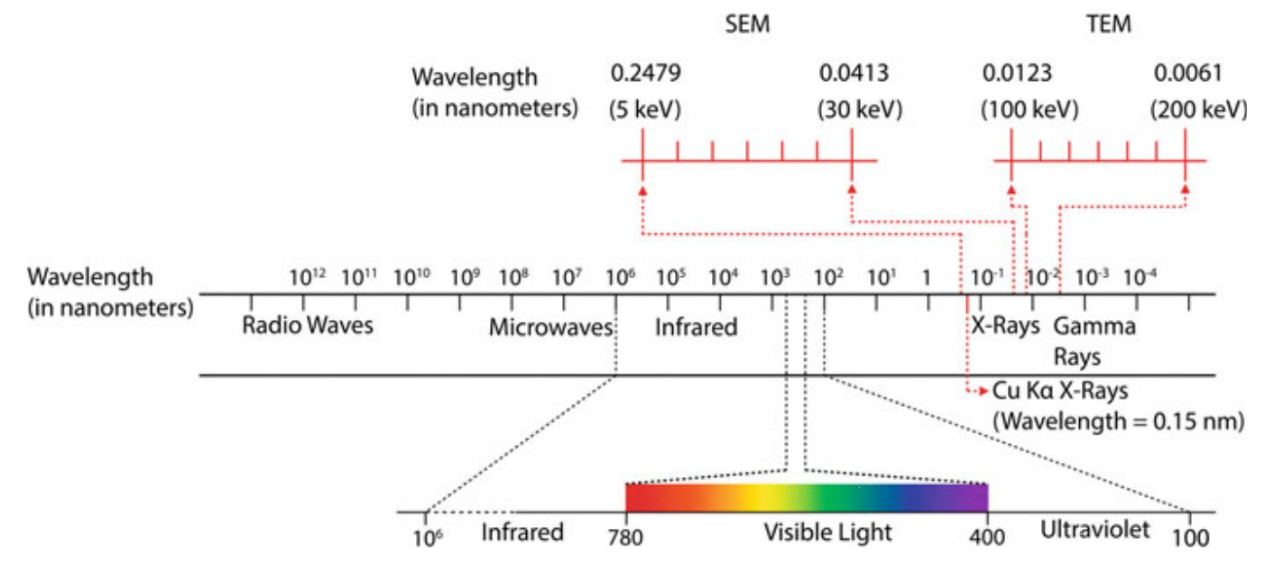
A Scanning Electron Microscope (SEM) is an analytical instrument that uses a focused beam of high-energy electrons to scan the surface of a specimen, producing high-resolution images at the nanometer scale.
Unlike optical microscopes that rely on light and glass lenses, SEM takes advantage of the extremely short wavelength of electrons, allowing it to reveal surface structures with far greater depth and clarity.
Beyond imaging, SEM can also provide chemical and crystallographic information through complementary detectors such as Energy Dispersive X-ray Spectroscopy (EDS) for elemental analysis and Electron Backscatter Diffraction (EBSD) for crystal orientation and phase mapping. This makes SEM indispensable in both academic research and industrial applications — from semiconductors and metallurgy to ceramics, polymers, and biological materials.
In essence, SEM bridges the gap between the microscopic and the nanoscopic worlds, enabling scientists and engineers to not only see the surface of matter but also understand its behavior at the most fundamental level.
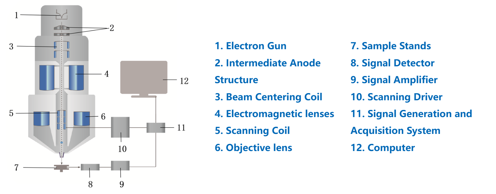
The operation of an SEM begins with the Electron Gun (1), which emits a focused beam of high-energy electrons. These electrons are accelerated and pass through the Intermediate Anode (2) to control their energy and trajectory. The Beam Centering Coil (3) ensures the beam is aligned along the optical axis of the microscope.
Next, the beam passes through a series of Electromagnetic Lenses (4) that act like magnetic “optics,” focusing the electrons into a fine probe with a nanometer-scale diameter. The Scanning Coil (5) then deflects the beam in a raster pattern across the specimen’s surface, line by line, allowing the system to collect signal data point by point.
When the electrons strike the sample on the Sample Stage (7), various signals are generated — primarily Secondary Electrons and Backscattered Electrons — which are detected by the Signal Detector (8). These signals are amplified by the Signal Amplifier (9) and processed through the Scanning Driver (10) and Signal Acquisition System (11).
Finally, the processed signals are displayed on the Computer (12) as an image, where variations in signal intensity correspond to differences in surface topography and composition. The result is a detailed, high-resolution image revealing the microscopic structure of the material’s surface.