FE SEM
CIQTEK FE-SEM – มองเห็นเหนือขีดจำกัดของความละเอียด
กล้องจุลทรรศน์อิเล็กตรอนแบบส่องกราดชนิดปล่อยสนาม (FE-SEM) ของ CIQTEK มอบการถ่ายภาพความละเอียดระดับอัลตร้าสูง พร้อมความเสถียรของปืนอิเล็กตรอนแบบ Schottky Field Emission ออกแบบมาสำหรับงานวิจัยวัสดุขั้นสูง อุตสาหกรรมสารกึ่งตัวนำ นาโนเทคโนโลยี และวิทยาศาสตร์ชีวภาพ โดยให้ความคมชัดเหนือชั้นทั้งที่แรงดันเร่งสูงและต่ำ เหมาะอย่างยิ่งสำหรับตัวอย่างที่บอบบางหรือไม่นำไฟฟ้า
- Ultra-High Resolution – ให้ความละเอียดสูงสุดถึง 0.6 นาโนเมตร ที่ 15 kV และ 1.0 นาโนเมตร ที่ 1 kV ช่วยให้สังเกตโครงสร้างระดับนาโนได้อย่างคมชัดน่าทึ่ง
- Low-Voltage Imaging Excellence – ลดการสะสมประจุของตัวอย่างและลดความเสียหายจากลำอิเล็กตรอน ด้วยระบบออปติก “Super-Tunnel” และเทคโนโลยีชะลอลำอิเล็กตรอนแบบคู่ (Dual Beam Deceleration)
- In-Lens & Multi-Detector System – ติดตั้งตัวตรวจจับแบบ In-Lens, Everhart-Thornley (ETD), BSE แบบเลื่อนเข้าออกได้, STEM และตัวเลือกเสริมอื่น ๆ เพื่อการถ่ายภาพและการวิเคราะห์ที่หลากหลาย
- Low Vacuum Capability – สังเกตตัวอย่างที่นำไฟฟ้าไม่ดีหรือไม่นำไฟฟ้าได้อย่างเสถียรโดยไม่ต้องเคลือบผิว ให้ความละเอียดสูงถึง 1.5 นาโนเมตร ที่ 30 kV ภายใต้โหมดสุญญากาศต่ำ
- Analytical Power – รองรับการขยายระบบสำหรับ EDS, EBSD, WDS และ CL เพื่อการวิเคราะห์โครงสร้างและองค์ประกอบอย่างครบถ้วน
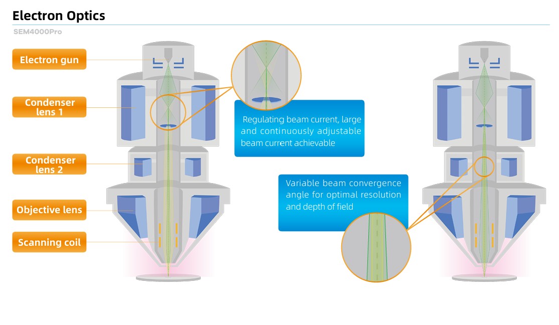

CIQTEK SEM4000Pro is an analytical FE-SEM with a high-brightness, long-life Schottky electron gun.
Its three-stage electromagnetic lens ensures superior performance for EDS/EDX, EBSD, WDS, and more.
With low-vacuum mode and advanced detectors, it excels at imaging non-conductive specimens.

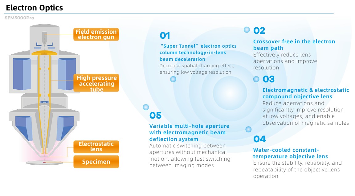
CIQTEK SEM5000Pro is a high-resolution Schottky FE-SEM with advanced “Super-Tunnel” electron optics.
It delivers crossover-free beam paths, minimized aberrations, and reduced charging effects.
Achieving 1.1 nm at 1 kV, it enables clear imaging of non-conductive samples with minimal damage.

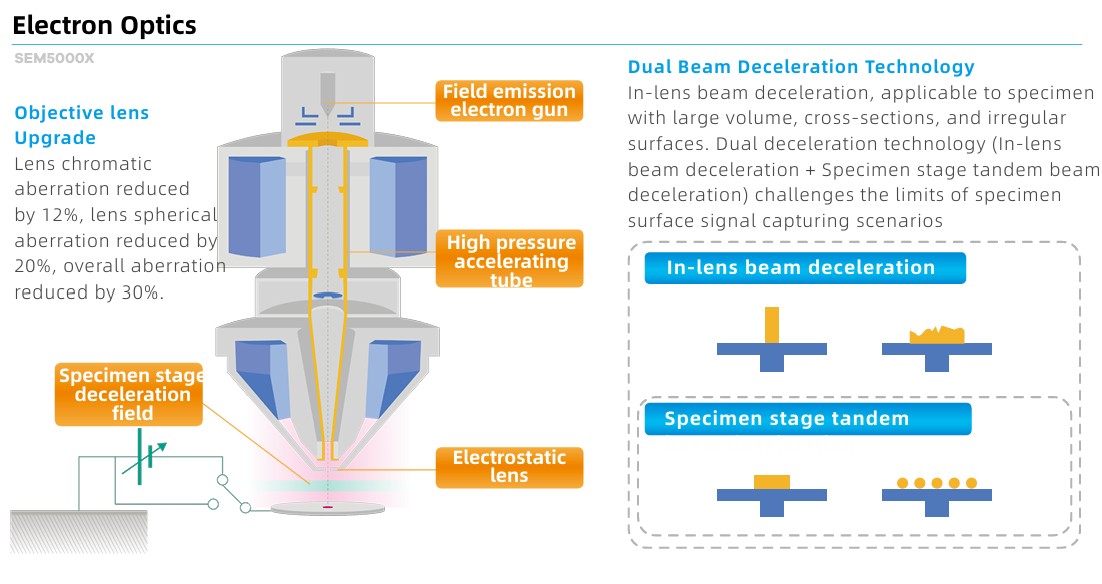
The CIQTEK SEM5000X is an ultra-high resolution FESEM with optimized electron optics column design, reducing overall aberrations by 30%, achieving ultra-high resolution of 0.6 nm@15 kV and 1.0 nm@1 kV. Its high resolution and stability make it advantageous in advanced nano-structural materials research, as well as the development and manufacturing of high-technology node semiconductor IC chips.
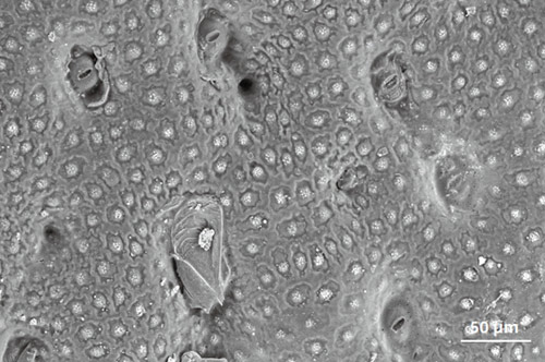
Pineapple Skin, Low Vacuum 100 Pa / 10 kV / BSED
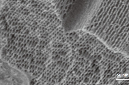
The pore structure of SBA-15 silica-based mesoporous material characterization, In-lens electron detector image at 500 V low voltage without conductive coating (under dual deceleration mode with In-lens beam deceleration + specimen stage tandem beam deceleration).
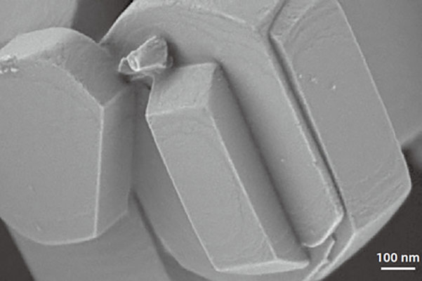
ZSM-8 molecular sieve, a typical catalyst across multiple frontier research fields. Low-voltage imaging without conductive coating provides direct characterization of the surface details of the molecular sieve particles.